


Compound chemical materials for 3D printing refer to a diverse class of advanced materials that combine two or more substances, often synthetic polymers, to create formulations with tailored properties for additive manufacturing processes. These materials go beyond traditional plastics and metals, encompassing composites, ceramics, and even bioinks, designed to expand the functionality and application scope of 3D printing. They are engineered to enhance properties such as strength, flexibility, thermal stability, conductivity, or biocompatibility, depending on the intended use.
Customizable Properties: By blending different chemicals and fillers, these materials can be designed to have specific mechanical, electrical, thermal, or optical characteristics.
Enhanced Performance: Compound materilas often outperform single single-component materials in terms of strength, heat resistance, or chemical resistance.
Functional Integration: They can incorporate functional elements like conductive fillers (e.g., carbon nanotubes) for electronics or biological components for tissue engineering.
Process Compatibility: Tailored to work with various 3D printing technologies, from Fused Deposition Modeling (FDM) to Stereolithography (SLA) and Inkjet Printing.
Sustainability: Some compounds incorporate recycled or bio-based materials, contributing to eco-friendly and sustainable manufacturing practices.
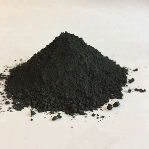
(3D printing vacuum annealing furnace for Compound semiconductor wafers)
The parameters of a 3D printing vacuum annealer can vary depending on the specific type of furnace being used, as well as the desired process and final product. However, some common parameters that may be important to consider include: * Temperature: The temperature at which the vacuum is generated and maintained can affect the rate of chemical reactions and the properties of the deposited material. * Pressure: The pressure of the vacuum can also impact the rate of chemical reactions and the properties of the deposited material. * Heat source: The heat source used in the vacuum Annealer can determine the direction and strength of the process, as well as the resulting physical changes in the deposited material. * Material type: The type of material being deposited and annealed will affect the required parameters, such as melting point, glass transition temperature, and thermal stability. * Annealing time: The amount of time spent in the vacuum Annealer can influence the degree of plasticity and crystallinity in the deposited material. Overall, selecting appropriate parameters for a 3D printing vacuum annealer will depend on the specific requirements of the desired process and the properties of the deposited material. It may be necessary to conduct experiments or consult with experts in the field to optimize these parameters for a given application.
(3D printing vacuum annealing furnace for Compound semiconductor wafers)
Advanced Manufacturing: Aerospace and automotive parts that require lightweight yet strong materials, such as carbon fiber reinforced thermoplastics for structural components.
Electronics: 3D printable conductive inks and resins for circuitry, sensors, and antennas, enabling rapid prototyping and customization in electronic device manufacturing.
Biomedical: Bioinks combining cells with supportive hydrogels for tissue engineering, organ modeling, and drug testing, pushing the boundaries of personalized medicine.
Consumer Products: Customized products with unique functionalities, such as flexible or color-changing materials for fashion, sports equipment, and home appliances.
Energy: Advanced battery and energy storage components, like solid-state electrolytes or porous structures for fuel cells, developed using compound chemical materials.
Company Profile
Kmpass is a trusted global chemical material supplier & manufacturer with over 12-year-experience in providing super high-quality 3D printing powder and relative products.
The company has a professional technical department and Quality Supervision Department, a well-equipped laboratory, and equipped with advanced testing equipment and after-sales customer service center.
If you are looking for high-quality 3D printing materials and relative products, please feel free to contact us or click on the needed products to send an inquiry.
Payment Methods
L/C, T/T, Western Union, Paypal, Credit Card etc.
Shipment
It could be shipped by sea, by air, or by reveal ASAP as soon as repayment receipt.
Q: Is 3D printing vacuum annealing furnace for Compound semiconductor wafers more expensive than standard 3D printing materials? A: Generally, yes, due to its specialized formulations and enhanced properties. However, cost varies widely depending on the material composition and application.
Q: Can all 3D printers handle compound chemical materials? A: No, compatibility depends on the type of material and the printer technology. Some materials may require specific printer settings or hardware modifications.
Q: Is 3D printing vacuum annealing furnace for Compound semiconductor wafers safe for users and the environment? A: Safety depends on the specific chemicals used. Many are developed with safety in mind, but it's crucial to follow handling guidelines and ventilation requirements.
Q: How do I choose the right compound material for my project? A: Consider the required end-use properties (mechanical, thermal, electrical), compatibility with your printer, and any regulatory or environmental constraints.
(3D printing vacuum annealing furnace for Compound semiconductor wafers)


